

3D Printed Music for your Ears
Part 2: Print'n Plate Series

tl;dr
We 3D printed and then copper plated planar coils and turned them into a working bluetooth speak!
Alrighty, so after a substantial hiatus, it’s probably time for an update. Last time we wrote, we had setup a sweet little process to produce 3D printed copper circuitry and had some blinking LEDs 🙄 . As you may well remember the technique, while reliable, depended heavily on placing special holes for small rivet pins. These pins helped conduct current and ensure that it was evenly distributed over the conductive filament circuit to get smooth and even copper deposition.
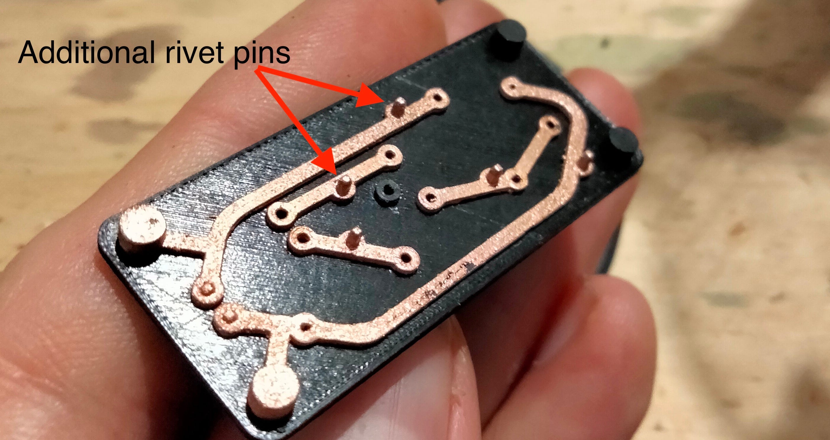
While the rivet pins enabled us to get some quality plated circuits, they had some significant limitations. The pins added complexity both in the plating setup and the 3D printing. The pins quickly became finicky to place and wire together, it always resulted in a dangling mess of wires. We experimented with “gold plated” pogo pin style setups but nothing worked as well as the embedded rivet pins. These pins also didn’t scale well for circuits that had very long traces, like coils. We almost always ended up having to have a pin hole every 3-4 cm of coil length!
Additionally, they reduce the minimum trace width we could print because printing the through holes gets significantly less accurate as the diameter of those holes shrink. Needless to say the pins approach was non-trivial to automate and we needed a rethink…
A New Technique
As luck would have it, we got a number of interesting ideas while chatting on twitter after the initial post. One of the more exciting ideas was suggested by @mechadense. It boiled down to a conductive plane backed onto the circuit which would ensure each point of the circuit was at the same potential relative to the anode.
A Backplane Sandwich?
By printing the circuit completely through we could expose the underside of it. This underside of the circuit could be connected to the large conductive backplane. One can see the original idea in the below diagram. This solution was great as it solved the problem of making sure every part of the circuit had enough current density and meant we could plate faster and more evenly.
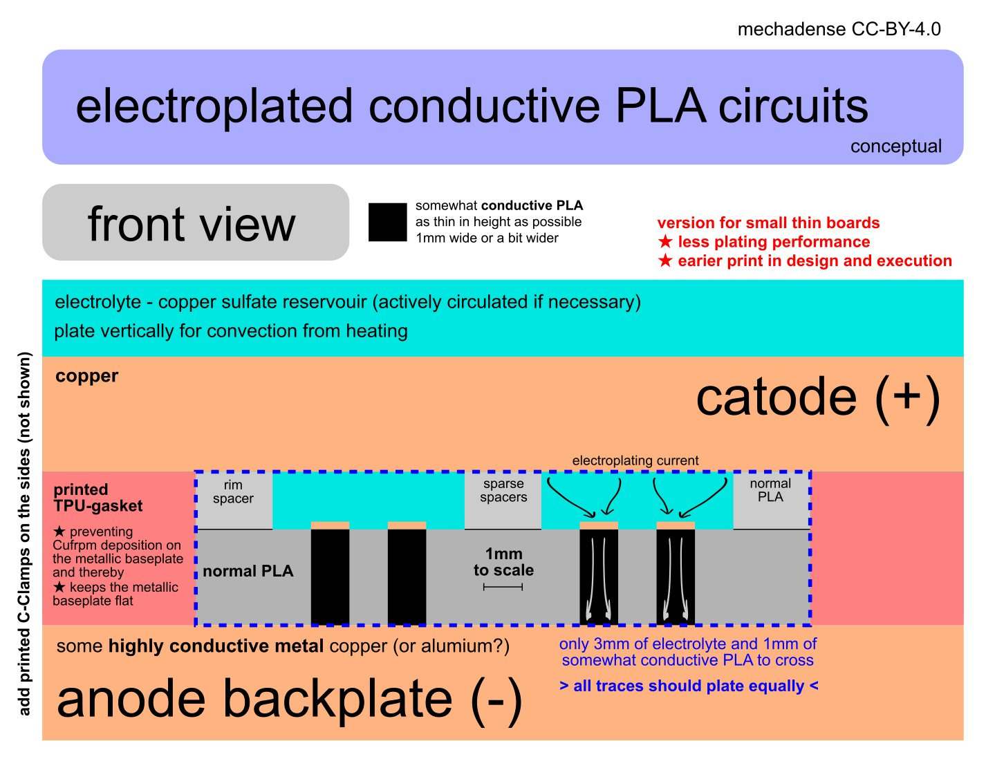
This was a great addition and the backplane was so much more efficient than previous methods. We didn’t even need to place the positive copper anode so close or introduce the actively circulated ducts of electrolyte. So we stripped back the initial design a bit and produced something which was potentially a little more straightforward to automate and prove out the concept.
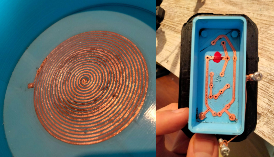
Cup Plating
Enter the idea of “cup plating”…

Above was our first iteration. The basic idea is to print your circuit all the way through so that it can back onto the conductive Cathode. You then need to enclose the circuit in a water tight cup. The advantage of this method is that we minimise the current flow path and it can potentially be printed and plated in place. The current only need travel through the depth of the conductive PLA trace and the electrolyte solution gap to the anode. With this design, this distance is fairly similar for every single point on the circuit. Additionally, we can probably make it even more so by optimising the size and position of the anode.
This initial iteration did uncover several downsides or caveats with the design, namely:
One needs to design a cup structure into the circuit model and this needs some post processing to remove.
The whole print needs to be water tight, this can be difficult to achieve. It also places a limit on the thickness of the PCB one can produce. If we made be PCB too thin, it almost always leaked. It’s frustrating to get things water tight with FDM printing!
Through holes are no longer possible without a post process to drill them out.
However, the largest problem we found with this design was that it was non-trivial to get a good consistent contact between the cathode backplate and the bottom of the print.
Initially we thought it would be amazing to have the backplane cathode actually be our 3D printers hotbed. Since we already have the print backed onto the bed and we could easily programmatically apply current there if it were conductive. Unfortunately, this proved pretty difficult and we were unable to get even semi-reasonable adhesion to the smooth spring steel sheets we had on hand. Unsurprisingly, any of the coated sheets didn’t conduct electricity so they were out too. We also tried to print directly onto aluminium foil, but that was only marginally better and prints would pull off after a layer or two. A conductive print bed might still be a good approach if we could find an etched aluminium or copper build plate, although one might still run into problems when the build plate cools down during plating and it looses contact with the print.
A final desperate attempt to get the cup method working was to use conductive graphite spray paint on blue painters tape. While we could easily print our cup with this method, the graphite paint proved to be too weakly conductive, but it lead to the current iterations design.
Conductive Rafts
Our current cup plating method now incorporates a large conductive PLA raft which is removable after plating.

From our previous experiments on how infill affects conductivity, we knew that a larger more densely packed raft would provide the best base. In our successful builds, we used a 10 layer raft with 100% infill. One of the more difficult parameters to dial in was the raft interface gap. If it was too large, the print would end up being less water tight. Conversely it it was too small, the print would bond too tightly to the raft and not be removable.
Now, with the backplate being conductive PLA, the connection to the power supply became very important. Previously, we had found that the interface between conductive PLA and metal is critical to the conductivity of the piece. One either needs a lot of force or to melt the connection into the PLA. For the majority of our tests we used heat-set inserts melted into the raft. This allowed us to anchor a solid connection to the negative cathode.

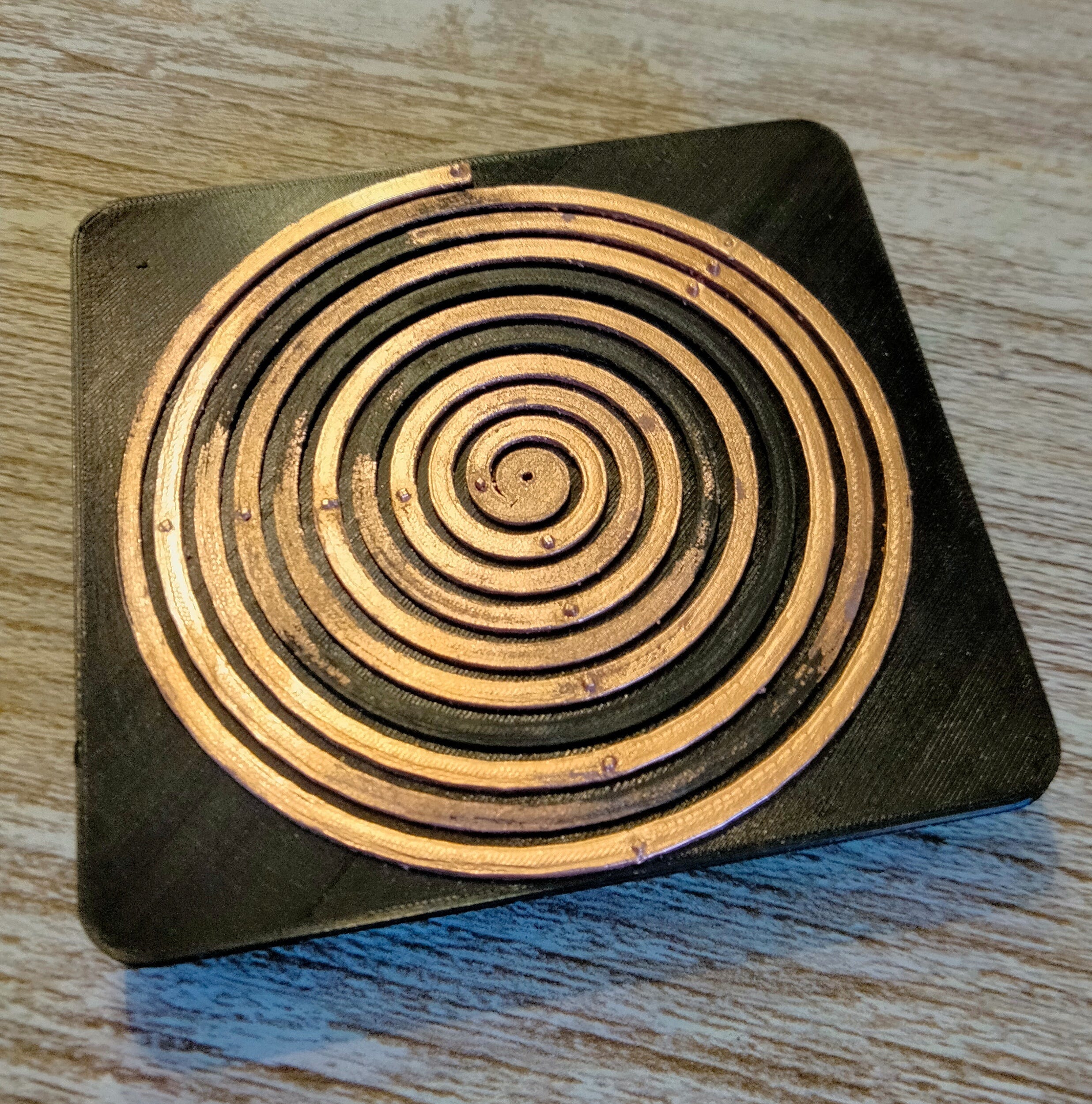
With these new improvements we approximately halved the plating time and were able to plate much longer coils. Below you can see a close up of the 20-turn coil and our trusty LED blinker circuit. Unfortunately, we don’t yet have the equipment to more closely inspect the quality and thickness of the plating.
One additional interesting thing to notice on the coil above is that the copper is actually inlayed into the blue PLA rather than embossed and sticking out like all our previous circuits and coils. This minor change seems to improve the thickness of the deposition as the copper somewhat builds up in the corners of the valley like trace. It also seemed to improve the water tightness of the bottom layer a bit as we could make the surrounding blue PLA portion thicker. This change still needs further testing and tweaking to figure out what depth of trace is best.
Sweet! Now can we do something useful?
So now we can make pretty decent circuits and planar coils, but can they actually be used for anything remotely useful? The most obvious first stop for a coil is to try make a small electro magnet. So we grabbed a raspberry pi and a Pimoroni motor driver board, cobbled together some basic python and started pumping current through our 20-turn coil.

This actually worked remarkably well and nothing set on fire. I think we were lucky the motor driver limits current to 1A. That seems to have kept things reasonable. In any case we were able to happily flick small neodymium magnets around all day. Great success!!
Since we have coils and magnets, we aren’t very far from having a little audio speaker. So that was the next challenge. We print’n plated a second coil (30-turns) and hooked the two coils up to an Adafruit Speaker Bonnet. We then placed each coil cup above a large neodymium magnet centred behind the coil. To make things easier and more fun we flashed the balenaSound project onto our Pi. This combo gave us a working stereo Spotify connect speaker right out the box. The audio quality is not going to knock any socks off but I can’t believe it works so well. Amazing!!!😍
Next Up: Motors?
So now we can make usable planar coils and have proved we can do useful thing with them like move magnets. So we are a good way towards printing a motor of some kind, but this technique is not without fault. There are a number of things we need to improve before we can make motor coils. These of some of the current issues we need to solve:
Printing a water tight cup is not simple with FDM. One can create fairly water tight cups by reducing the layer height to 0.1 - 0.15 mm and experimenting with different slicer settings. However, we found that often a cup that proved to be water tight was not actually “electrolyte tight”. It seems that the acidic nature of the electrolyte solution would possibly corrode small gaps or thin sections that the water would not. Currently, we brush a solvent called Dichloromethane onto the inside of the cup and this solvent seals up any of the gaps. However, Dichloromethane is a very nasty chemical and an alternative would be preferred.
We also found that if we made the coil trace with less than two nozzle widths wide (i.e.: 0.8mm for a 0.4mm nozzle) this would result in a very leaky cup. We are not 100% sure why, but it could be something slicer related in the way it places single extrusion width walls with no overlay with adjacent extrusions. This is unfortunate because that trace width limit reduces our ability to make smaller coils and we think more dense coils will allow for better motors…
Finally, the current setup seems to collects a lot of debris on the coil as plating proceeds, this results in nodules and non-smooth plates. This should be easily fixable by adding a small fibre cloth bag around the anode to trap debris.
Nothing insurmountable and we think even in the current state we will start trying to make some basic planar stepper or BLDC motors and just see how they do.
not sure if you have access to a resin printer to play with, in addition to an FDM printer?
they have such nice resolution and accuracy.
if you do, this concept might be worth looking into.
https://www.sciencedirect.com/science/article/abs/pii/S2214860421007375
just a thought. I have yet to delve into conductive plastics myself, but find your work extremely interesting.